
Part B:
1.To Display “Hello World” message using Internal UART.
Theory:
LPC1768 has four inbuilt USARTs numbering 0-3. similarly, the pins are also named as RXD0-RXD3 and TXD0-TXD3 respectively.
As the LPC1768 pins are multiplexed with multiple functionalities to reduced the pin count and to have a small form factor, first they have to be configured as UART pins.


Bit 7 – DLAB: Divisor Latch Access Bit
This bit is used to enable the access to divisor latch.
0-- Disable access to divisor latch
1-- Enable access to divisor latch


now lets discuss only UART0.
Explanation:
#include<LPC17xx.h>
void delay(unsigned int r1);
void UART0_Init(void);
void UART0_IRQHandler(void);
unsigned long int r=0, i = 0;
unsigned char tx0_flag=0;
unsigned char *ptr, arr[] = "Hello world";
int main(void)
{
SystemInit();
SystemCoreClockUpdate();
UART0_Init();
while(1)
{
ptr = arr;
while ( *ptr != '\0'){
LPC_UART0->THR = *ptr++;
while(tx0_flag == 0x00);
tx0_flag = 0x00;
for (i=0; i<200; i++);
}
for (i=0; i<500; i++)
delay(625); //delay
}
}
void UART0_Init(void)
{
LPC_SC->PCONP |= 0x00000008; //UART0 peripheral enable
LPC_PINCON->PINSEL0 |= 0x00000050; //for selecting TX0[P0.2-->5:4] and RX0[P0.3-->7:6] of UART0
LPC_UART0->LCR = 0x00000083; //enable divisor latch, parity disable, 1 stop bit, 8bit word length line control register
LPC_UART0->DLM = 0X00;
LPC_UART0->DLL = 0x13; //select baud rate 9600 bps
LPC_UART0->LCR = 0X00000003;
LPC_UART0->FCR = 0x07;
LPC_UART0->IER = 0X03; //select Transmit and receive interrupt
NVIC_EnableIRQ(UART0_IRQn); //Assigning channel
}
void UART0_IRQHandler(void)
{
unsigned long Int_Stat;
Int_Stat = LPC_UART0->IIR; //reading the data from interrupt identification register
Int_Stat = Int_Stat & 0x06; //masking other than txmit int & rcve data indicator
if((Int_Stat & 0x02)== 0x02) //transmit interrupt
tx0_flag = 0xff;
}
void delay(unsigned int r1)
{
for(r=0;r<r1;r++);
}
Download:Internal UART
1.To Display “Hello World” message using Internal UART.
Theory:
LPC1768 has four inbuilt USARTs numbering 0-3. similarly, the pins are also named as RXD0-RXD3 and TXD0-TXD3 respectively.
As the LPC1768 pins are multiplexed with multiple functionalities to reduced the pin count and to have a small form factor, first they have to be configured as UART pins.

fig: Uart0,1,,2 & 3 and its corresponding PortPins

fig: UART Registers
LCR ( Line Control Register ):
This register is used for defining the UART frame format ie. Number of Data bits, STOP bits.

Bit 1:0 – WLS : WordLenghtSelect
These two bits are used to select the character length
00-- 5-bit character length
01-- 6-bit character length
10-- 7-bit character length
11-- 8-bit character length
These two bits are used to select the character length
00-- 5-bit character length
01-- 6-bit character length
10-- 7-bit character length
11-- 8-bit character length
Bit 2 – Stop Bit Selection:
This bit is used to select the number(1/2) of stop bits
0-- 1 Stop bit
1-- 2 Stop Bits
This bit is used to select the number(1/2) of stop bits
0-- 1 Stop bit
1-- 2 Stop Bits
Bit 3 – Parity Enable:
This bit is used to Enable or Disable the Parity generation and checking.
0-- Disable parity generation and checking.
1-- Enable parity generation and checking.
This bit is used to Enable or Disable the Parity generation and checking.
0-- Disable parity generation and checking.
1-- Enable parity generation and checking.
Bit 5:4 – Parity Selection:
These two bits will be used to select the type of parity.
00-- Odd parity. Number of 1s in the transmitted character and the attached parity bit will be odd.
01-- Even Parity. Number of 1s in the transmitted character and the attached parity bit will be even.
10-- Forced "1" stick parity.
11-- Forced "0" stick parity
Bit 6 – Break Control
0-- Disable break transmission.
1-- Enable break transmission. Output pin UARTn TXD is forced to logic 0
0-- Disable break transmission.
1-- Enable break transmission. Output pin UARTn TXD is forced to logic 0
Bit 7 – DLAB: Divisor Latch Access Bit
This bit is used to enable the access to divisor latch.
0-- Disable access to divisor latch
1-- Enable access to divisor latch
Baudrate Calculation
LPC1768 generates the baud rate depending on the values of DLM,DLL.
Baudrate = PCLK/ (16 * ( 256 * DLM + DLL) * (1+ DivAddVal/MulVal))
Baudrate = PCLK/ (16 * ( 256 * DLM + DLL) * (1+ DivAddVal/MulVal))
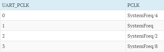
Getting the PCLK value.
PCLKSELx registers contain the PCLK info for all the clock dependent peripherals in which Bit6,Bit7 contains the Uart Clock(ie.UART_PCLK) information.
The UART_PCLK and the actual Peripheral Clock(PCLK) is calculated as below.
(Refer data sheet for more info)
PCLKSELx registers contain the PCLK info for all the clock dependent peripherals in which Bit6,Bit7 contains the Uart Clock(ie.UART_PCLK) information.
The UART_PCLK and the actual Peripheral Clock(PCLK) is calculated as below.
(Refer data sheet for more info)
DivAddVal/MulVal == 0
Using the above parameters , DLL/DLM is calculated as below.
(256 * DLL + DLM) = PCLK / (16* Baudrate).
(256 * DLL + DLM) = PCLK / (16* Baudrate).
Baud =
PCLK in Hertz16 x (256xDLM + DLL) x (1 + DIVADDVAL/MULVAL)
Where DIVADDVAL & MULVAL are part of “Fractional Rate Divider” or “Baud-Prescaler” which is used in Baud-Rate generation. This “Fractional Divider” is only active when DIVADDVAL > 0. This formula is pretty common for LPC ARM micro-controllers.
which can be further simplified to :
Baud =
MULVALMULVAL + DIVADDVAL
X
PCLK in Hertz16 x (256xDLM + DLL)
with following conditions strictly applied:
- 0 < MULVAL <= 15
- 0 <= DIVADDVAL <= 14 - if DIVADDVAL > 0 & DLM = 0 then, DLL must be >= 2
- DIVADDVAL < MULVAL
Where PCLK is the Peripheral Clock value in Hz , DLM and DLL are the divisor registers
PCLK in Hertz16 x (256xDLM + DLL) x (1 + DIVADDVAL/MULVAL)
MULVALMULVAL + DIVADDVAL
X
PCLK in Hertz16 x (256xDLM + DLL)
1) The Dirty and Simplest Method:
The quickest and also the dirtiest(accuracy wise) method without using any algorithm or fine-tuning is to set DLM=0 and disable the Fractional Divider. In this case MULVAL=1 and DIVADDVAL=0 which makes the Fraction Part(FP) = 1. Now we are left with only 1 unknown in the equation which is UxDLL and hence we simplify the equation and solve for UxDLL.
UxDLL =
PCLK in Hertz16 x Desired-BaudRate
In my opinion, if possible, you must stay away from above method as it works only for particular bauds & specific PCLK value and moreover computed UxDLL might get out of range i.e. > 255 in which case you have to start increasing DLM and recompute a new value for DLL.
FCR ( FIFO Control Register )
LPC1768 has inbuilt 16byte FIFO for Receiver/Transmitter. Thus it can store 16-bytes of data received on UART without overwriting. If the data is not read before the Queue(FIFO) is filled then the new data will be lost and the OVERRUN error bit will be set.

UART0-->IER [interrupt Enable Register]
Set a bit to 0 to disable and 1 to enable the corresponding interrupt. Other bits are reserved.
- Bit 0 – RBR Interrupt Enable
- Bit 1 – THRE Interrupt Enable
- Bit 2 – RX Line Status Interrupt Enable

IIR – Interrupt Identification Register: This register is organized as follows:
- Bit 0 – Interrupt Pending 0 means at-least one interrupt is pending, 1 means no interrupts are pending. [Note: This bit is ACTIVE LOW!]
- Bits [3 to 1] – Interrupt Identification : [011] implies Receive Line Status(RLS) , [010] implies Receive Data Available(RDA) , [110] implies Character Time-out Indicator(CTI) , [001] implies THRE Interrupt.
- Bits [7 to 6] – FIFO Enable.
Explanation:
#include<LPC17xx.h>
void delay(unsigned int r1);
void UART0_Init(void);
void UART0_IRQHandler(void);
unsigned long int r=0, i = 0;
unsigned char tx0_flag=0;
unsigned char *ptr, arr[] = "Hello world";
int main(void)
{
SystemInit();
SystemCoreClockUpdate();
UART0_Init();
while(1)
{
ptr = arr;
while ( *ptr != '\0'){
LPC_UART0->THR = *ptr++;
while(tx0_flag == 0x00);
tx0_flag = 0x00;
for (i=0; i<200; i++);
}
for (i=0; i<500; i++)
delay(625); //delay
}
}
void UART0_Init(void)
{
LPC_SC->PCONP |= 0x00000008; //UART0 peripheral enable
LPC_PINCON->PINSEL0 |= 0x00000050; //for selecting TX0[P0.2-->5:4] and RX0[P0.3-->7:6] of UART0
LPC_UART0->LCR = 0x00000083; //enable divisor latch, parity disable, 1 stop bit, 8bit word length line control register
LPC_UART0->DLM = 0X00;
LPC_UART0->DLL = 0x13; //select baud rate 9600 bps
LPC_UART0->LCR = 0X00000003;
LPC_UART0->FCR = 0x07;
LPC_UART0->IER = 0X03; //select Transmit and receive interrupt
NVIC_EnableIRQ(UART0_IRQn); //Assigning channel
}
void UART0_IRQHandler(void)
{
unsigned long Int_Stat;
Int_Stat = LPC_UART0->IIR; //reading the data from interrupt identification register
Int_Stat = Int_Stat & 0x06; //masking other than txmit int & rcve data indicator
if((Int_Stat & 0x02)== 0x02) //transmit interrupt
tx0_flag = 0xff;
}
void delay(unsigned int r1)
{
for(r=0;r<r1;r++);
}
No comments:
Post a Comment